|
 |
 |
Atmospheric Pressure Plasma CVD |
|
|
|
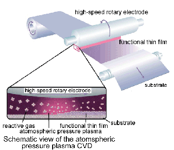
| The atmospheric pressure plasma chemical vapor deposition (AP-PCVD) is a new ultrahigh-rate deposition technique in which atmospheric pressure, very high frequency (VHF) plasma is utilized. By employing a high-speed rotary electrode, the deposition rate and homogeneity of thin films can be markedly improved in comparison with those fabricated by conventional low-pressure plasma CVD. Particles generated in the plasma, which degrade the film quality, are easily removed from the plasma area along with the high-speed gas flow. In addition, it is possible to make a film with a large area by scanning a substrate. |
 |
| |
| At present, we are researching the ultrahigh-rate deposition of various functional materials such as amorphous silicon (a-Si) and polycrystalline silicon (poly-Si) films for solar cell devices, epitaxial silicon films for semiconductor device substrates, silicon carbide films for micro- and opto-electronic devices operating under severe conditions, and high-functional thin films for liquid crystal displays. |
| |
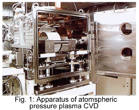
Figure 1 shows the AP-PCVD apparatus. The apparatus consists of the reaction chamber, the load lock chamber and the gas circulation system for removing particles generated in the plasma. To maintain cleanliness of the process atmosphere, the motor drives and all of the bearings, which contain organic lubricant, are placed outside the chamber using magnetic coupling except that of the electrode shaft. A local area around the bearings of the electrode shaft is evacuated to avoid organic contamination in the chamber.
Using the AP-PCVD, it becomes possible to deposit an a-Si film of 300nm thickness with a 1m x 1m area in approximately 200 seconds (the average deposition rate: 1.5nm/s) at a substrate scanning speed of 5mm/s, if a rotary electrode wider than 1m is used. The deposition rate is more than 10 times faster than that of low-pressure plasma CVD. From the various research results, both an extremely high deposition rate and excellent film property can be simultaneously obtained by the AP-PCVD, which is very attractive for the mass production of a-Si solar cells.
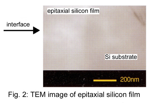
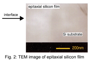
Figure 2 shows an example of the low-temperature and high-rate deposition of epitaxial silicon films. A reduction in the deposition temperature by more than 500℃ and an increase in the deposition rate by a factor of 20 in comparison with those in industrial thermal CVD are simultaneously achieved. |
| |
 |
 |
|