Center for Atomistic Fabrication Technology, Osaka University
Home Site Map Japanese
Message from the Program Leader
The 21st Century COE Program
Overview
Image
Research Promotion Personnel
Atomistic Fabrication Technology
What is Atomistic Fabrication Technology?
EEM
Plasma CVM
Atmospheric Pressure Plasma CVD
Electro-chemical processing using only ultrapure water
Ultra-precision Aspheric Surface Measurement
SREM/STM
Ultra-weak Light Scattering Surface Measurement
Ab initio (first principal) Molecular Dynamics Simulation
Research Presentation
Scientific Papers
International Conferences
Other
Information
SREM/STM(Scanning Reflection Electron Microscopy/ Scanning Tunneling Microscopy)

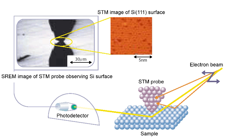
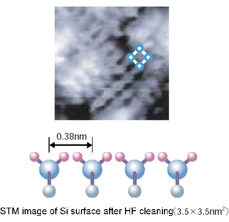
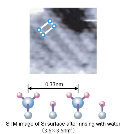
For the fabrication of electronic and optical devices in the 21st century, the topographic structures of surfaces after various processes such as ultraprecision machining, thin-film growth and wet cleaning must be measured in the wide range of spatial resolution from meters to nanometers.We have to evaluate the flatness, crystallinity and defects of such surfaces.For example, various nanometer-scaled functional devices must be guaranteed to operate perfectly on a Si wafer (φ=300mm).Furthermore, the atomic-scale control of surfaces structures in a large area is required for optical devices such as highly accurate X-ray mirrors.

 
SREM/STM (scanning reflection electron microscopy/ scanning tunneling microscopy) is used to observe and evaluate surface atomic structures in the spatial resolution from micrometers to nanometers. At first, terraces and steps are observed by SREM. Then the local area to be investigated in detail is determined in the SREM image, and the STM probe is moved into the position. Atomic images by STM enable us to evaluate the atomic arrangement of the local area determined by SREM.
 
The right figure shows a schematic drawing of SREM/STM observations. The screening of an electron beam by the STM probe induces the black shadow in the SREM image. This shadow enables us to recognize the position of the probe. The surface atomic structure beneath the probe in the SREM image is magnified in the STM image. Each surface atom is clearly resolved. The STM images shown below are examples of Si surfaces after wet cleaning. These wet cleaning processes have an important role in the fabrication of semiconductor devices. We have succeeded in observing clear atomic images after wet cleaning of Si(001) surfaces for the first time in the world. We have demonstrated that the atomic arrangements of Si surfaces strongly depend on cleaning procedures.
 
 
All Rights Reserved. Copyright (c) 2003 Osaka University.