|
 |
 |
EEM |
|
|
|
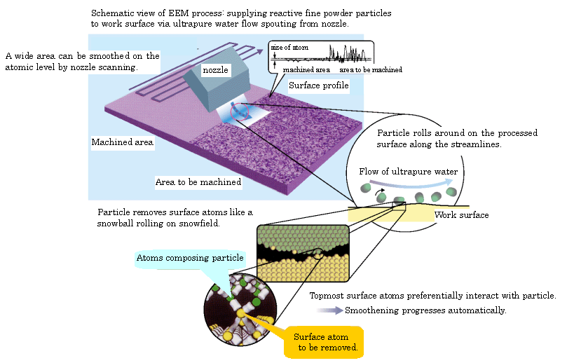
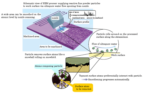
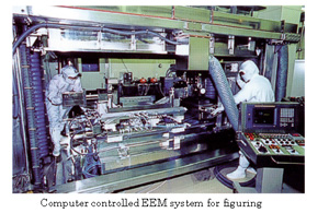
| EEM is an ultraprecision machining process utilizing chemical reactions between solid surfaces. Atom removal in EEM proceeds in the following ways. When two solid surfaces come into contact with each other and then separate, there is a notable probability that the atoms of one surface will adhere to the other surface. Fine powder particles, of which surfaces have reactivity to the target material, are employed as working solids in the processing. As shown in the first figure, they are uniformly mixed with ultrapure water and transported to the processed surface via the controlled flow of ultrapure water using a nozzle-type scanning head. Then, the particles roll around on the processed surface along the streamlines and preferentially remove the topmost atoms on the surface like snowballs rolling on a snowfield. |
| |
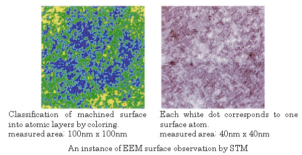
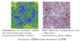
| The second figure shows scanning tunneling microscopy (STM) images of an EEM-processed Si(001) surface, the scanned areas of which are 100nm x 100nm and 40nm x 40nm. Each atomic layer is colored in the first image to see the degree of flatness. In the second one, which is a zoomed-up image of the first one, all surface atoms are found to be placed on crystallographically reasonable positions, and no distorted areas are observed. As seen in the colored image, nearly 95% in relation to the entire area is composed of only three atomic layers. This is the flattest surface in the world prepared by a method other than heating in ultrahigh vacuum. Ultraprecision figuring of the required shape with an accuracy higher than 1nm in peak-to-valley can also be performed by scanning the nozzle head under suitable feed-speed maps because EEM processing proceeds in the spatially small area in which the nozzle head is facing. |
| |
 |
 |
| |
| SPring-8, which is a 3rd-generation synchrotron radiation facility, brings highly coherent X-ray beams to advanced scientific instrumentations in many fields such as physics, biology and life science. However, an ultraprecise mirror for steering coherent X-ray beams has not been realized and is highly demanded. Unprecedented degrees of surface smoothness and figure accuracy are required for coherent X-ray optics. We are trying to materialize such mirrors using EEM and plasma CVM processes, which have been developed by us. The applicability of these fabrication methods has already been confirmed under the collaboration with the X-ray optics group of SPring-8/RIKEN. |
 |
| |
|