Center for Atomistic Fabrication Technology, Osaka University
Home Site Map Japanese
Message from the Program Leader
The 21st Century COE Program
Overview
Image
Research Promotion Personnel
Atomistic Fabrication Technology
What is Atomistic Fabrication Technology?
EEM
Plasma CVM
Atmospheric Pressure Plasma CVD
Electro-chemical processing using only ultrapure water
Ultra-precision Aspheric Surface Measurement
SREM/STM
Ultra-weak Light Scattering Surface Measurement
Ab initio (first principal) Molecular Dynamics Simulation
Research Presentation
Scientific Papers
International Conferences
Other
Information
Ultra-weak Light Scattering Surface Measurement
A measuring system for nanoparticles with diameters on the nanometer (nm) order scale on a Si wafer surface has been developed. As shown in the left figure, when a focused laser beam is scanned on a Si wafer and a spot of the laser beam passes through a particle and a defect, scattered light is generated. The intensity of scattered light depends on the sizes of the particle and defect. When the intensity of scattered light as a voltage is measured using a photo multiplier tube (PMT) and a CR circuit, the sizes of the particle and defect are estimated with an accuracy on the nanometer order.


Measuring system using light scattering method.


Principle of measurement.


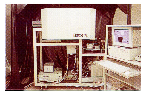
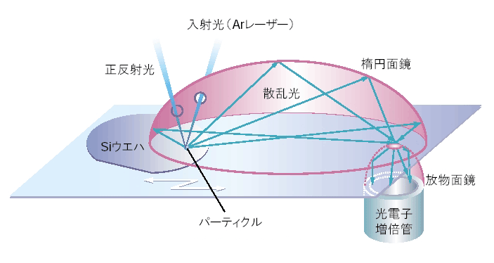
The minimum detectable size for particles is 50nm at best in a conventional particle counter. In this new measuring system, all scattered light can be guided to the PMT using the ellipsoidal and parabolic reflectors. At the same time, background light is eliminated as much as possible, which makes it possible to measure scattered light corresponding to a particle with a diameter of 25 nm. Our developed measuring system is able to detect defects such as scratches of namometer order width and microroughness, as well as particles of namometer order diameter on a Si wafer surface.

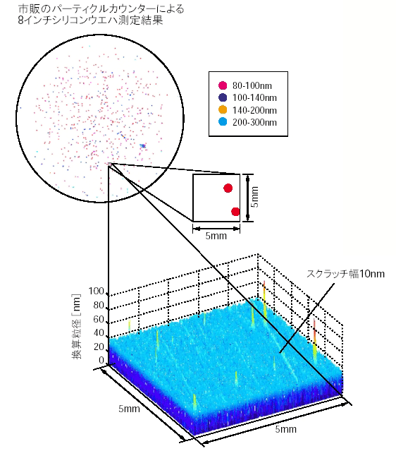
The middle left figure shows the result of measured particles on the surface of an 8-inch Si wafer with a conventional particle counter. The bottom left figure shows the result in an area of 5mm×5mm on the same Si wafer with the developed measuring system. It turns out that our system can detect particles with diameters smaller than 50nm, which is difficult to accomplish with the conventional particle counter. In addition, this system is able to measure nanostructures on the surface, such as scratches of approximately less than 10 nm in width.


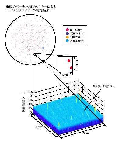
Measured results of particles and scratches on Si wafer (5mm x 5mm) by our developed system.

 
All Rights Reserved. Copyright (c) 2003 Osaka University.